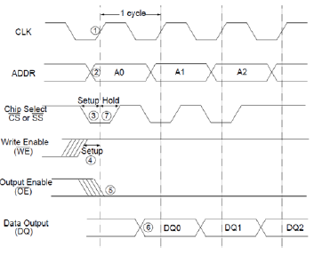
Given the timing diagram below which is derived from the data sheet of a commercial SRAM, explain its action in words.

Timing diagram of a SRAM memory
This is a read cycle because the write enable signal, WE*, is inactive?high (i.e., negated) for three cycles. The key event is the assertion of the active?low chip select, CS*, on the rising edge of the first clock. When CS* goes active low, an access is triggered. Note that CS* must go low before the rising edge of the clock (setup
time) and remain low until the hold time after the rising edge.
The write enable must be high before the rising edge of the clock for its setup time to recognize a read cycle. Similarly, the output enable, OE*, must become active?low before the rising edge of the clock. If WE* remains high and OE* low, then data is put on the data bus in each clock cycle. In each case the address must be valid
before each rising edge of the clock.
You might also like to view...
If you use the Expression Builder, you still need to manually separate field names and table names with exclamation points
Indicate whether the statement is true or false
Adding a sum to a field in the subreport causes the sum to display in the subreport control on the main form
Indicate whether the statement is true or false